TinkerBench is reader-supported. When you buy through links on our site, we may earn an affiliate commission.
DIY PCB Etching: A Step-by-Step Guide for Hobbyists
Phone cases · 15% off first order
Phone Case GiftThey pick the model · 2 minutes Code FIRST15GIFT
Creating your own printed circuit boards (PCBs) at home can seem daunting, but it’s a rewarding skill for any electronics enthusiast. Instead of waiting weeks for a board house, you can iterate quickly and prototype designs in your own workshop. This guide will walk you through the entire PCB etching DIY process, from design to finished board, covering essential materials, safety precautions, and proven etching techniques. We’ll focus on methods suitable for hobbyists, prioritizing affordability and accessibility.
Why Etch Your Own PCBs?
There are several compelling reasons to learn PCB etching:
- Faster Prototyping: Eliminate the lead time of ordering boards online, allowing you to test and refine your designs much more quickly.
- Cost Savings: For simple boards and small quantities, etching can be cheaper than professional fabrication.
- Customization: You have complete control over the board layout and materials.
- Learning Experience: The process provides valuable insight into PCB manufacturing.
- Emergency fixes: Sometimes you just need to fix something now.
Who is this guide for?
This guide is perfect for intermediate hobbyists with some basic electronics knowledge and access to a well-ventilated workspace. Beginners with very simple needs can use this guide; professionals requiring high-precision, multi-layer boards should stick to professional PCB fabrication services.
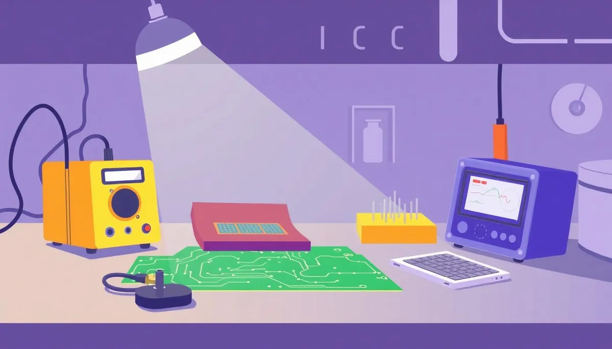
Materials and Equipment Checklist
Before you begin, gather the following materials and equipment. Safety gear is non-negotiable.
Essential Materials
- Copper-Clad Boards: Single-sided or double-sided FR-4 boards. Size depends on your project.
- Laser Printer: For printing your PCB layout onto transparency film. Inkjet will NOT work.
- Transparency Film: Special transparent sheets designed for laser printers.
- Photoresist Developer: Sodium carbonate (washing soda) is a common and effective option.
- Photoresist Etchant: Ferric chloride is a reliable and readily available etchant. Ammonium persulfate is another option, but requires more precise temperature control.
- UV Light Source: A UV exposure unit or even direct sunlight can be used to expose the photoresist.
- Isopropyl Alcohol (IPA): For cleaning the boards.
- Distilled Water: For rinsing. /products/b004cqrg0a-fiji-natural-artesian-bottled-water-1-liter-33-8-fl-oz-pack/Check on Amazon → or any other clean source.
Essential Equipment
- Etching Tank or Container: A plastic container (Tupperware works well) to hold the etchant.
- Agitation System: A rocking platform, bubbler, or manual agitation to speed up etching.
- Heater (Optional): An aquarium heater can help maintain a consistent etchant temperature (around 40-50°C for ferric chloride).
- Timer: For accurately timing exposure and etching.
- Gloves (Nitrile or Rubber): Protect your hands from chemicals.
- Safety Glasses: Protect your eyes from splashes.
- Ventilation: A well-ventilated workspace is crucial. A fume hood is ideal, but working outdoors or near an open window is often sufficient.
- PCB Drill: A small drill press or rotary tool with PCB drill bits.
- Cleaning Supplies: Paper towels, sponges, etc.
- Bright Light Source: For inspecting the etched board. /products/b005fegyco-lighting-ever-led-flashlights-high-lumens-small-flashlight-w/Check on Amazon →
Software
- PCB Design Software: KiCad, Eagle, or Altium Designer are popular options. KiCad is free and open-source.
Step-by-Step PCB Etching Process
Phone cases · 15% off first order
Titan CasePrecision fit · 2,000+ designs Code FIRST15TIT
Follow these steps carefully to create your own PCBs:
1. Design Your PCB
- Use your chosen PCB design software to create your board layout.
- Ensure your traces are wide enough to carry the intended current (use online calculators for this).
- Double-check your design for errors before proceeding.
- Print your layout onto transparency film using a laser printer. Print at the highest resolution possible, and make sure the black ink is opaque. Some people print two copies of the layout and align them to further increase opacity.
2. Prepare the Copper-Clad Board
- Clean the copper surface thoroughly with isopropyl alcohol and a clean cloth or paper towel.
- Handle the board by the edges to avoid contaminating the surface with fingerprints.
3. Apply Photoresist (If Using Pre-Sensitized Boards)
- Many copper-clad boards come pre-coated with a photoresist layer. If yours does, skip this step.
- If not, you’ll need to apply photoresist using a spray or dipping method. This is more complex and requires careful technique to achieve an even coating. Pre-sensitized boards are highly recommended for beginners.
4. Expose the Photoresist
- Place the transparency film (with the printed layout) onto the photoresist-coated board. Ensure the black ink side is in direct contact with the photoresist.
- Use a UV light source to expose the photoresist. The exposure time will vary depending on the light source and the photoresist used. Start with a test strip to determine the optimal exposure time. A good starting point is 5 minutes with a dedicated UV exposure unit or 15-30 minutes in direct sunlight.
- Overexposure will result in overly thin traces, while underexposure will prevent the photoresist from developing properly.
5. Develop the Photoresist
- Prepare the developer solution. For sodium carbonate, a concentration of about 1% (10g per liter of water) is a good starting point.
- Immerse the exposed board in the developer solution and gently agitate.
- The unexposed photoresist will dissolve, revealing the copper underneath.
- Rinse the board thoroughly with distilled water.
- Inspect the board carefully. If any areas are not fully developed, repeat the developing process for a short time.
6. Etch the Copper
- Prepare the etchant solution. Follow the manufacturer’s instructions for mixing ferric chloride or ammonium persulfate.
- Preheat the etchant to the recommended temperature (around 40-50°C for ferric chloride).
- Immerse the board in the etchant solution and agitate gently.
- The etchant will dissolve the exposed copper, leaving behind the copper traces protected by the photoresist.
- Monitor the etching process closely. The etching time will vary depending on the etchant concentration, temperature, and agitation. A good starting point is 15-30 minutes.
- Remove the board from the etchant when all the exposed copper is gone.
- Rinse the board thoroughly with distilled water.
7. Remove the Photoresist
- Use a solvent such as acetone or isopropyl alcohol to remove the remaining photoresist.
- Clean the board thoroughly.
8. Drill Holes
- Use a PCB drill or rotary tool with PCB drill bits to drill the necessary holes for components.
- Use the correct drill bit size for each component lead.
9. Inspect and Test
- Inspect the board carefully for any defects, such as broken traces or shorts.
- Use a multimeter to check for continuity and shorts.
- Test the board with your circuit to ensure it functions correctly.
Safety Precautions
Etching PCBs involves working with hazardous chemicals. Always follow these safety precautions:
- Wear Safety Glasses: Protect your eyes from splashes.
- Wear Gloves: Protect your hands from chemicals.
- Work in a Well-Ventilated Area: Avoid inhaling fumes. A fume hood is ideal.
- Dispose of Chemicals Properly: Do not pour etchant down the drain. Follow local regulations for hazardous waste disposal.
- Read Material Safety Data Sheets (MSDS): Understand the hazards of each chemical you are using.
- Keep Children and Pets Away: Store chemicals out of reach of children and pets.
- Neutralize Acids: Have baking soda (sodium bicarbonate) on hand to neutralize acid spills.
Troubleshooting
Phone cases · 15% off first order
Phone Cases For CharityEvery case supports a cause Code GIVE10
- Uneven Etching: This can be caused by uneven agitation, inconsistent etchant temperature, or poor contact between the transparency film and the photoresist.
- Broken Traces: This can be caused by overexposure, underexposure, or using too much force when handling the board.
- Shorts: This can be caused by incomplete etching, solder bridges, or debris on the board.
- Poor Photoresist Adhesion: This can be caused by insufficient cleaning of the copper surface.
Alternatives to Traditional Etching
While the above method is the most common, several alternatives exist:
- Laser Toner Transfer: Print the layout onto special transfer paper and iron it onto the copper-clad board. The toner acts as an etch resist.
- CNC Milling: Use a CNC milling machine to remove the unwanted copper. This is a more precise and repeatable method.
- Direct Inkjet Printing: Use a specialized inkjet printer with conductive ink to print the circuit directly onto the board. This is the most advanced and expensive option.
Conclusion
DIY PCB etching is a valuable skill for any electronics hobbyist. By following this guide and taking the necessary safety precautions, you can create your own PCBs at home and bring your electronic projects to life. Remember to start with simple designs and practice your technique. Over time, you’ll develop the skills and experience needed to create more complex and sophisticated boards. Don’t be afraid to experiment and learn from your mistakes. And always prioritize safety!